Have you ever imagined your smartphone or tablet without a touchscreen? This could soon be the case if we run out of indium, one of the rarest minerals on Earth.
Indium is used in many high-tech devices such as touch screens, smartphones, solar panels, and smart windows, in the form of indium tin oxide. This compound is optically transparent and electrically conductive — the two crucial features required for touch screens to work.
But there’s a problem: we have no guaranteed long-term supply of indium. It is naturally found only in tiny traces and is therefore impractical to mine directly. Almost all of the world’s indium comes as a byproduct of zinc mining.
Fortunately, we have a potential solution: my colleagues and I have developed a new way to make optically transparent and electrically conductive coatings without indium.
A worsening problem
Because the world’s indium supply is tied to zinc mining, its availability and price will depend on the demand for zinc.
Possible declines in zinc demand — already evident in the car manufacturing industry — along with the ever-increasing usage of smartphones and touch panels — are set to exacerbate the potential shortage of indium in the future.
One option is to try and recycle indium. But recovering it from used devices is expensive because of the tiny amounts involved.
When a crucial material is in short supply, we should look for alternatives. And that’s exactly what my colleagues and I have found.
How does it work?
Our new coating, details of which are published in the journal Solar Energy Materials and Solar Cells, involves plasma technology.
Plasma is like a soup of charged particles in which electrons have been ripped away from their atoms, and is often described as the fourth state of matter, after solid, liquid, and gas. It might sound like an exotic substance, but in fact, it comprises more than 99% of the visible objects in the universe. Our Sun, like most stars, is essentially a giant ball of glowing plasma.
Closer to home, fluorescent light bulbs and neon signs also contain plasma. Our new touchscreen films don’t contain plasma, but their manufacture uses plasma as a way to create new materials that would otherwise be impossible to make.
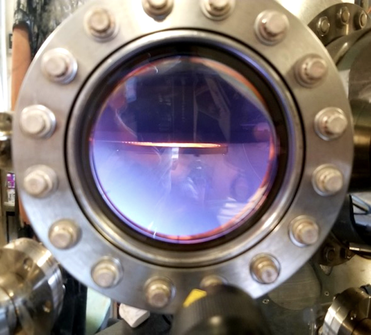
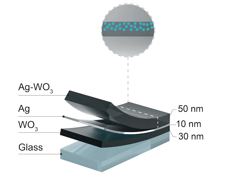
Our coating is made of an ultra-thin layer of silver, sandwiched between two layers of tungsten oxide. This structure is less than 100 nanometres thick — roughly one-thousandth of the width of a human hair.
These ultra-thin sandwich layers are created and coated onto glass using a process called “plasma sputtering”. This involves subjecting a mixture of argon and oxygen gases to a strong electric field until this mixture transforms into the plasma state. The plasma is used to bombard a tungsten solid target, detaching atoms from it and depositing them as a super-thin layer onto the glass surface.
We then repeat this process using silver, and then a final third time tungsten oxide embedded with silver nanoparticles. The entire process takes only a few minutes, produces minimal waste, is cheaper than using indium, and can be used for any glass surface such as a phone screen or window.
The finished plasma coating also has another intriguing feature: it is electrochromic, meaning it can become more or less opaque, or change color if an electrical voltage is applied.
This means it could be used to create super-thin “printable displays” that can become dimmer or brighter, or change color as desired. They would be flexible and use little power, meaning they could be used for a range of purposes including smart labels or smart windows.
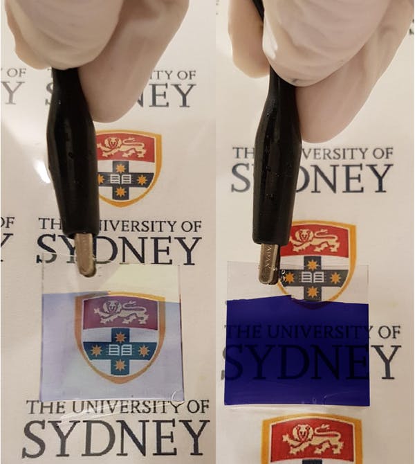
Our new indium-free technology holds great potential to manufacture the next-generation touch-screen devices such as smartphones or electronic papers, as well as smart windows and solar cells for environmental sustainability. This technology is ready to be scaled up for creating coatings on commercial glass, and we are now doing further research and development to adapt them for future wearable electronic devices. Smart windows coated with our new films could be used to block the flow of light and thus heat as required. Our plasma film can be applied to any glass surface, which can then be set to adjust its transparency depending on the weather outside. Unlike existing “photochromic” spectacle lenses, which respond to ambient light levels, our material responds to electrical signals, meaning it can be manipulated at will.
Article by Behnam Akhavan, Senior Lecturer, ARC DECRA Fellow, School of Biomedical Engineering and School of Physics, University of Sydney
This article is republished from The Conversation under a Creative Commons license. Read the original article.
Get the TNW newsletter
Get the most important tech news in your inbox each week.
